| Frequency band | 9XXMHz for US915/AU915/KR920/AS923 |
| AI | Analog Input |
| ANT_SW | RP2040: GPIO25; Function: SX1262 RF switch power |
| AO | Analog Output |
| AVDD | Pin No.: 46; Type: PI; Description: ADC Reference Voltage |
| BUSY | RP2040: GPIO15; Function: SX1262 BUSY |
| DI | Digital Input |
| DIO1 | RP2040: GPIO29; Function: SX1262 DIO1 |
| DO | Digital Output |
| DVDD | Pin No.: 45; Type: PI; Description: Supply for the MCU |
| ESD_CDM | Description: Charged Device Model; Min.: -; Nom.: -; Max.: 500; Unit: V |
| ESD_HBM | Description: Human Body Model; Min.: -; Nom.: -; Max.: 2000; Unit: V |
| GND | Pin No.: 14, 17, 23, 37, 40, 44; Type: Ground; Description: Ground |
| GPIO22 | Pin No.: 27; Type: IO; Description: General-purpose input/output |
| GPIO23 | Pin No.: 28; Type: IO; Description: General-purpose input/output |
| GPIO24 | Pin No.: 29; Type: IO; Description: General-purpose input/output |
| GPIO26; ADC1 | Pin No.: 43; Type: IO; AI; Description: General-purpose input/output; General-purpose ADC interface |
| GPIO27 | Pin No.: 41; Type: IO; Description: General-purpose input/output |
| GPIO28; ADC0 | Pin No.: 44; Type: IO; AI; Description: General-purpose input/output; General-purpose ADC interface |
| GPIO7 | Pin No.: 11; Type: IO; Description: General-purpose input/output |
| GPIO8 | Pin No.: 12; Type: IO; Description: General-purpose input/output |
| GPIO9 | Pin No.: 13; Type: IO; Description: General-purpose input/output |
| I2C1_SCL | Pin No.: 5; Type: DO; Description: I2C serial clock |
| I2C1_SDA | Pin No.: 4; Type: IO; Description: I2C serial data |
| I2C2_SCL | Pin No.: 25; Type: DO; Description: I2C serial clock |
| I2C2_SDA | Pin No.: 24; Type: IO; Description: I2C serial data |
| IO | Bidirectional |
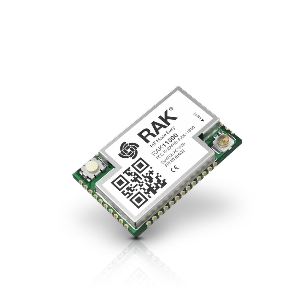
| Model | RAK11300 |
| NRESET | RP2040: GPIO14; Function: SX1262 reset |
| Operating Temperature | Minimum: -20; Typical: 25; Maximum: 85; Unit: ° C |
| PI | Power Input |
| PO | Power Output |
| RAK11300 | UART, USB |
| RAK11300(H) | Region: Europe; Frequency: EU868; Region: America; Frequency: US915; Region: Australia; Frequency: AU915; Region: Korea; Frequency: KR920; Region: Asia; Frequency: AS923; Region: India; Frequency: IN865; Region: Russia; Frequency: RU864 |
| RAK11300(L) | Region: Europe; Frequency: EU433; Region: China; Frequency: CN470 |
| Reset | Pin No.: 18; Type: DI; Description: Reset the module, Active Low |
| RF_LoRa | Pin No.: 38; Type: IO; Description: LoRa antenna interface; Comment: 50 Ω Impedance; This pin can' t be used on modules with an IPEX connector. If unused, keep this pin open. |
| SPI0_CSN | Pin No.: 35; Type: DO; Description: SPI chip select |
| SPI0_MISO | Pin No.: 33; Type: DI; Description: SPI master input, slave output |
| SPI0_MOSI | Pin No.: 34; Type: DO; Description: SPI master output. slave input |
| SPI0_SCK | Pin No.: 30; Type: DO; Description: SPI clock |
| SPI_MISO | RP2040: GPIO12; Function: SPI Master in |
| SPI_MOSI | RP2040: GPIO11; Function: SPI Master out |
| SPI_NSS | RP2040: GPIO13; Function: SPI select |
| SPI_SCK | RP2040: GPIO10; Function: SPI clock |
| Storage Temperature | Minimum: -20; Maximum: 85; Unit: ° C |
| SWCLK | Pin No.: 19; Type: Debug; Description: SWD clock input for debugging and programming |
| SWDIO | Pin No.: 20; Type: Debug; Description: SWD I/O for debugging and programming |
| UART1_RX | Pin No.: 9; Type: DI; Description: UART1 receive |
| UART1_TX | Pin No.: 10; Type: DO; Description: UART1 transmit |
| UART2_RX | Pin No.: 6; Type: DI; Description: UART2 receive |
| UART2_TX | Pin No.: 7; Type: DO; Description: UART2 transmit |
| USB_DM | Pin No.: 2; Type: IO; Description: USB differential data(-) |
| USB_DP | Pin No.: 3; Type: IO; Description: USB differential data(+) |
| VBAT_SX | Pin No.: 21; Type: PI; Description: Supply for the LoRa IC |
| VBAT_SX_IO | Pin No.: 22; Type: PI; Description: Supply for the Digital I/O interface pins |
| Wireless technologies | LoRa |